
Introduction
The metallic finish on a cosmetic compact, the scratch-resistant coating on a cutting tool, and the transparent conductor layer inside a smartphone display may share one manufacturing secret: magnetron sputtering. Despite its widespread use, engineers, designers, and procurement professionals often encounter the term without a clear picture of how it works, which variant suits their needs, or why it outperforms older methods.
Industry projections put the global sputtering equipment market at $2.41 billion in 2025, growing to $4.19 billion by 2035 at a 5.83% CAGR — a trajectory driven by demand across semiconductors, optics, automotive, and consumer goods. That breadth of adoption makes understanding the process increasingly relevant for anyone specifying or sourcing surface coatings.
This guide covers the core physics, the main process types, a side-by-side comparison with competing methods, and the industries where magnetron sputtering delivers the greatest value.
Key Takeaways
- Magnetron sputtering uses plasma and magnetic fields to eject atoms from a target and deposit ultra-thin films on substrates
- Magnetic electron trapping boosts plasma density and deposition rates compared to conventional sputtering
- Main variants—DC, RF, reactive, pulsed, HiPIMS—suit different materials and performance goals
- High film purity, strong adhesion, and low substrate temperatures let manufacturers coat heat-sensitive parts without distortion
- Industries from semiconductors to cosmetics rely on magnetron sputtering for precise, durable coatings
What Is Magnetron Sputtering and How Does It Work?
Magnetron sputtering is a Physical Vapor Deposition (PVD) technique where energetic argon ions bombard a solid target, ejecting atoms that travel across a vacuum chamber and condense on a substrate. Those atoms form the thin film. The term "magnetron" refers to the horseshoe-magnet assembly positioned behind the target — the component that confines electrons near the target surface and drives ionization efficiency.
The Role of the Magnetic Field
The magnetic field traps secondary electrons in helical paths near the target surface, dramatically increasing the probability of ionizing collisions with argon atoms. This produces a dense plasma at lower pressures (1–15 mTorr) and voltages than conventional diode sputtering, which required higher operating pressures and suffered from lower deposition rates.
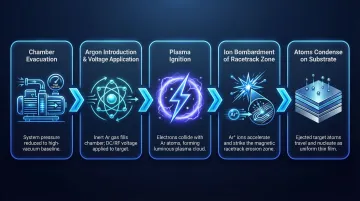
Step-by-Step Deposition Sequence
With that plasma established, the deposition sequence follows a predictable path:
- Chamber evacuation to high vacuum (base pressure typically <10⁻⁶ Torr)
- Argon introduction and application of high negative voltage to the cathode (target)
- Plasma ignition confined by the magnetic field near the target surface
- Ion bombardment of the target's "racetrack" erosion zone
- Neutral sputtered atoms crossing the vacuum and condensing on the substrate
Magnetron Geometry and Target Types
A magnetron cathode assembly consists of the target material and a permanent-magnet (or electromagnet) arrangement that creates orthogonal electric and magnetic fields. Common target geometries include:
- Planar circular – Standard for research and small-batch production
- Planar rectangular – Used for large-area coating of architectural glass
- Rotatable cylindrical – Preferred for high-volume manufacturing due to superior target utilization (75–90% vs. 25–40% for planar targets)
Historical Context
William Robert Grove published the earliest sputter deposition experiments in 1852. The planar magnetron cathode didn't follow until 1974, when John S. Chapin filed U.S. Patent 4,166,018. That patent unlocked the high deposition rates that made magnetron sputtering commercially viable — large-scale architectural glazing, for instance, became a practical application by the mid-to-late 1970s.
Types of Magnetron Sputtering
Magnetron sputtering comes in several configurations, each suited to different materials, film requirements, and production environments. Here's how the main types compare.
DC Magnetron Sputtering
A constant direct-current voltage is applied to a conductive target. This variant offers:
Advantages:
- Simple, cost-effective power supply
- High deposition rates for metals (Ti deposition scales from 2.28 nm/min at 200 W to ~35 nm/min at 600 W)
- Efficient for depositing aluminum, copper, titanium, and other conductors
Constraint:
- Requires electrically conductive targets; unsuitable for insulating materials without auxiliary techniques
When the target material is non-conductive, DC sputtering falls short — that's where RF sputtering takes over.
RF Magnetron Sputtering
Alternating the anode–cathode bias at radio frequency (13.56 MHz, an ITU-reserved ISM band) prevents charge build-up on insulating targets, enabling deposition of oxides, nitrides, and dielectrics.
Key characteristics:
- Typical deposition rate: ~15 nm/min at 3 kW for SiO₂
- Lower deposition rates compared to DC sputtering
- Requires expensive RF power supplies and impedance matching networks
- Essential for depositing ceramic and dielectric films
Reactive Magnetron Sputtering
Introducing a reactive gas (O₂, N₂, or hydrocarbon) alongside argon causes sputtered metal atoms to chemically react and form compound films—oxides, nitrides, carbides—on the substrate.
The main challenge is target poisoning: the Berg model describes hysteresis behavior where the target abruptly transitions between metallic and poisoned (compound) states. Without active control, this causes unpredictable jumps in deposition rate and film stoichiometry.
Mitigation strategies:
- Optical emission monitoring for real-time feedback
- Mid-frequency pulsed DC power supplies (20–350 kHz) to discharge poisoned areas and prevent arcing
- Careful partial pressure management
Pulsed Magnetron Sputtering and HiPIMS
Pulsed DC sputtering (20–350 kHz) solves arc formation when depositing dielectrics by periodically reversing polarity to discharge accumulated charge.
High-Power Impulse Magnetron Sputtering (HiPIMS) delivers pulses typically 50–200 µs wide at peak power densities reaching several kW/cm², achieving metal ionization fractions of 70–90%. This produces dense, smooth films with superior adhesion — used in:
- High-end cutting tools
- Optical layers requiring extreme uniformity
- Applications demanding superior adhesion
Trade-off: Lower average deposition rate compared to conventional DC due to ion back-attraction to the target during high-power pulses.
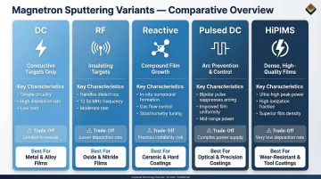
Closed Field Unbalanced Magnetron Sputtering (CFUBMS)
This configuration uses multiple magnetrons with magnetic field lines linked between cathodes, confining plasma across the substrate region for enhanced ion bombardment during film growth.
Applications:
- Graded multilayer coatings
- Diamond-like carbon (DLC) adhesion layers
- Corrosion-resistant alloy films requiring dense microstructures
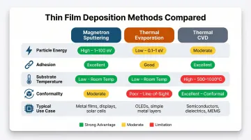
Magnetron Sputtering vs. Other Deposition Methods
| Feature | Magnetron Sputtering | Thermal Evaporation | Thermal CVD |
|---|---|---|---|
| Deposition Principle | Ion bombardment (momentum transfer) | Thermal energy vaporization | Chemical gas-phase reactions |
| Particle Energy | 1–100 eV | 0.1–0.5 eV | Thermal/chemical |
| Adhesion | Excellent | Weak/poor | Excellent |
| Substrate Temperature | <150–200 °C | Low to moderate | 450–800 °C |
| HAR Conformality | Poor (line-of-sight) | Very poor | Excellent |
| Typical Use Case | Metals, alloys, functional coatings | Pure metals, simple geometries | Dielectrics, semiconductors |
Each method has a different strength profile — the table above captures the technical tradeoffs, and the breakdown below shows where those differences actually matter in practice.
Where Magnetron Sputtering Wins
- Lower substrate temperatures than CVD, protecting polymers and flexible electronics
- Consistent alloy stoichiometry, unlike evaporation where vapor pressures vary between elements
- Higher particle energy (1–100 eV vs. 0.1–0.5 eV for evaporation) drives stronger film adhesion through inter-diffusion and mixing
- Deposits high-melting-point materials without melting them
Where Magnetron Sputtering Faces Limitations
- CVD and ALD provide better conformality on deep trenches and high-aspect-ratio features
- Evaporation delivers faster deposition rates for pure metals
- Large-area flat substrates may be more cost-effective with evaporation
If your parts involve complex geometries or deep features, CVD or ALD is worth the higher process temperature. For most metal and alloy coatings on flat or moderately shaped substrates, magnetron sputtering is the better fit.
Key Advantages of Magnetron Sputtering
High Deposition Rate with Minimal Substrate Heating
Magnetic confinement produces dense plasma at lower voltages, enabling rapid material transfer without thermally damaging temperature-sensitive substrates. Modern magnetron sputtering maintains substrate temperatures below 150–200 °C, making it suitable for polymers, flexible electronics, and other heat-sensitive materials.
Versatile Material Compatibility and Excellent Film Quality
Virtually any material that can be fabricated into a target—metals, alloys, ceramics, nitrides, oxides—can be sputtered. The resulting films exhibit:
- High purity
- Strong substrate adhesion due to energetic particle impact
- Small grain size
- Uniform thickness over large areas
That range covers everything from hard industrial coatings to the mirror-bright metallic finishes used in cosmetic packaging and automotive trim.
Precise, Repeatable Process Control
Key parameters can be independently tuned to dial in specific film properties:
- Power levels
- Pressure and gas composition
- Substrate bias voltage
- Magnetic field strength
- Substrate rotation speed
This level of control translates directly to consistent output at industrial scale, where batch-to-batch reproducibility determines whether a production run succeeds or fails.
Known Limitations of Magnetron Sputtering
Low Target Utilization and Frequent Replacement
The "racetrack" erosion pattern caused by the annular magnetic field concentrates ion bombardment on a narrow zone, leaving much of the target material unused. Planar targets typically achieve only 25–40% utilization, leading to:
- Higher material costs
- More frequent downtime for target replacement
- Wasted expensive target material (especially critical for precious metals)
Rotatable cylindrical targets address this directly. By continuously presenting fresh material to the plasma, they achieve 75–90% utilization and extend service intervals considerably. While rotatable targets carry higher upfront costs, their effective cost per utilized material runs roughly 60% of planar targets.
Target utilization is only one piece of the challenge. Reactive deposition introduces a separate set of process control problems.
Plasma Instability in Reactive Processes
Introducing reactive gases triggers competing reactions at the target surface — known as target poisoning — producing non-linear hysteresis behavior. The process can flip abruptly between metallic and compound sputtering modes, making consistent film composition difficult to maintain.
Modern industrial systems manage this through:
- Optical emission feedback control
- Mid-frequency pulsed DC power supplies (20–350 kHz)
- Careful partial pressure management with mass flow control valves
Key Industrial Applications of Magnetron Sputtering
Electronics, Semiconductors, and Data Storage
Magnetron sputtering deposits thin metal and dielectric films for:
- Integrated circuits (barrier layers like TiN and TaN, Cu seed layers)
- Gate dielectrics
- Passive components
- Sensor layers
- Touch screens
- OLED barrier layers (SiO₂/Al₂O₃ laminated films)
- Thin-film transistors
Historical applications include hard disk recording layers and CDs/DVDs. The sputtering equipment market's projected growth to $4.19 billion by 2035 is driven primarily by semiconductor fabrication, advanced displays, and data storage demands.
Automotive, Architectural, and Decorative Coatings
Automotive: CrN coatings on engine components reduce wear and friction. Decorative metallic finishes on plastic trim components deliver high-quality appearance without the environmental burden of traditional plating.
Architectural: Low-emissivity (Low-E) multilayer coatings on glass improve energy efficiency. Large-scale planar and rotatable magnetrons deposit silver layers sandwiched between dielectric films for high-performance glazing systems.
Decorative: PVD-based metallization is increasingly replacing hexavalent chromium electroplating. With EU REACH Annex XIV and RoHS restrictions phasing out carcinogenic Cr(VI), the automotive decorative chromium sector (67.13% market share in 2024) is rapidly transitioning to trivalent chromium and PVD alternatives.
Providence Metallizing Company has applied magnetron sputtering and PVD coatings — including titanium nitride, zirconium nitride, and chrome nitride — since the 1980s, offering over 30 distinct finishes on plastic substrates for cosmetic brands and industrial customers alike.
Energy, Biomedical, and Emerging Sectors
Thin-film solar cells:
- CIGS absorber layers (molybdenum back contacts deposited via sputtering)
- Transparent conductive oxides
- NiOₓ hole transport layers for perovskite solar cells
Biomedical implants:
- Calcium phosphate and hydroxyapatite coatings on titanium dental implants via RF magnetron sputtering enhance osseointegration
- Diamond-like carbon (DLC) coatings on orthopedic components reduce wear and extend implant lifespan
Emerging applications:
- Thin-film solid-state batteries
- Quantum computing components requiring ultra-precise nanoscale layers
Across all these sectors, the requirement is the same — films that are dense, well-adhered, and precisely controlled at the nanoscale. That combination of precision and throughput is what makes magnetron sputtering the process of choice for production environments.
Frequently Asked Questions
What is sputtering deposition?
Sputtering deposition is a PVD technique in which energetic ions (usually argon) bombard a solid target material, ejecting atoms that travel through a vacuum and condense on a substrate to form a thin film. It is a purely physical—not chemical—process.
What is a magnetron in sputtering?
A magnetron is the magnet assembly positioned behind the sputtering target that creates a closed magnetic field parallel to the target surface. It traps electrons in helical paths near the target, boosting plasma density for faster, more efficient sputtering at lower operating pressures.
What are the different types of magnetron sputtering?
The main variants include DC magnetron sputtering, RF magnetron sputtering, reactive magnetron sputtering, pulsed magnetron sputtering, HiPIMS, and CFUBMS. Each is suited to different materials (conductive vs. insulating) and application goals (deposition rate vs. film density).
How does RF magnetron sputtering work?
RF sputtering alternates the anode-cathode bias at 13.56 MHz, periodically discharging accumulated charge on insulating targets to prevent arcing. This allows oxides, nitrides, and other dielectric materials to be sputtered where DC methods would fail.
Is magnetron sputtering PVD or CVD?
Magnetron sputtering is a PVD (Physical Vapor Deposition) process because material transfer relies on physical momentum transfer from ion bombardment—not on chemical reactions of gaseous precursors as in CVD.
How long does a sputter target last?
Lifespan varies by power and target thickness, but the limiting factor is always the racetrack erosion groove — once it penetrates through, the target needs replacement. Planar targets achieve only 25–40% material utilization, while rotatable cylindrical targets reach 75–90%, lasting significantly longer and reducing effective material cost by roughly 40%.