Introduction
Plastic has become the dominant choice for modern electronic enclosures: it's lightweight, cost-effective, and offers design flexibility that metal can't match. But there's a critical challenge engineers face that metal enclosures never presented—plastic provides zero inherent electromagnetic interference (EMI) shielding. Every unprotected plastic enclosure is electromagnetically transparent, meaning interference flows freely in both directions: out from your device, and in from the surrounding environment.
This guide is for engineers, product designers, OEMs, and procurement teams who need to understand how conductive coatings transform plastic enclosures into effective electromagnetic shields. We'll cover the four primary coating methods—conductive spray/paint, vacuum metallizing (PVD sputtering), electroless plating, and electroplating—along with the critical design factors that determine real-world shielding performance.
The stakes are concrete: without proper EMI shielding, products risk failing regulatory certification (FCC Part 15, CE marking, MIL-STD-461), malfunctioning in electromagnetically dense environments, or emitting interference that disrupts surrounding electronics.
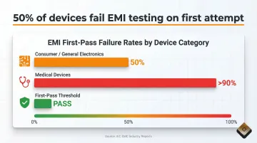
50% of devices fail EMI testing on the first attempt, and over 90% of medical devices miss first-pass compliance. Getting shielding right before you reach certification testing saves time, cost, and redesign cycles.
Key Takeaways
- Plastic has no natural electromagnetic shielding; conductive coatings create the necessary barrier
- Four shielding methods ranked by performance: spray coatings (60–90 dB), vacuum metallizing (up to 80 dB), electroless plating (>80 dB), and electroplating (highest)
- Performance hinges on coating uniformity, seam design, and keeping openings smaller than the critical wavelength
- Selection criteria: frequency range, production volume, substrate compatibility, and regulatory requirements
- Bring coating suppliers in during enclosure design — late-stage changes cost significantly more
Why Plastic Enclosures Need Conductive Coatings for EMI Shielding
Unmodified plastic is electromagnetically transparent—it neither reflects nor absorbs electromagnetic energy. Unlike metal enclosures that provide inherent shielding through reflection and absorption, plastic does nothing to stop interference from entering or escaping an enclosure.
That gap creates real problems at the product level:
- Regulatory compliance failures: Products fail FCC Part 15 or CISPR 32 emissions testing during certification
- Susceptibility to external interference: Devices malfunction in electromagnetically dense environments (hospitals, automotive systems, industrial settings)
- Field failures and recalls: Unshielded products may interfere with surrounding electronics or experience operational disruptions
According to Intertek Testing Services data, approximately 50% of devices fail initial EMI testing. For electrical medical devices, the failure rate exceeds 90%. Medical devices, telecommunications equipment, aerospace systems, automotive electronics, and consumer products all face strict EMC certification requirements—and a failed test means delayed launches, redesign costs, and retesting fees.
Types of EMI Shielding Coatings for Plastic Enclosures
Four well-established methods exist for making plastic enclosures conductive. Each suits different performance targets, production volumes, and enclosure geometries.
Conductive Spray Coatings and Paints
Conductive paints are the most accessible EMI shielding method. They incorporate conductive metal particles—typically silver, copper, nickel, or carbon—suspended in an acrylic or epoxy binder, applied to the interior surface of plastic enclosures.
Material performance:
- Silver: Highest conductivity. MG Chemicals 842 Silver Conductive Coating provides 72-85 dB shielding from 100 MHz to 1 GHz at 2.0 mil (50 µm) thickness
- Silver-coated copper: Balance of performance and cost. Parker Chomerics CHO-SHIELD 2056 delivers 70 dB shielding at 1 mil (25 µm) thickness
- Nickel: Lower cost with good corrosion resistance. MG Chemicals 841 provides 36-49 dB shielding from 100 MHz to 1 GHz at 2 mil thickness
Tradeoffs:
- Easy to apply to complex geometries
- Lower capital investment
- May exhibit lower shielding effectiveness at higher frequencies compared to plated coatings
- Adhesion quality depends heavily on surface preparation and binder chemistry
Vacuum Metallizing and PVD Sputtering
Vacuum metallizing (thermal evaporation) and PVD sputtering deposit thin, uniform metal films — commonly aluminum, copper, nickel, or alloys — onto plastic substrates in controlled vacuum environments. Sputtering offers high uniformity and strong adhesion, making it well-suited for high-frequency applications requiring consistent shielding across complex surfaces. The process deposits 1-5 µm metal layers through energized plasma that ejects atoms from a target material onto the substrate. Providence Metallizing Company has applied sputtered metal coatings for EMI-RFI applications since the 1980s, when the company introduced magnetron sputtering to its finishing capabilities.
Performance characteristics:
- Aluminum layers achieve 80 dB attenuation at gigahertz frequencies
- Multi-layer thin films (Cu, NiFe, NiFe/Cu) with 4 µm thickness show superior shielding effectiveness from 0.7 GHz to 10 GHz
- Minimal thickness adds negligible weight
- Excellent uniformity across complex geometries
Electroless Plating
Electroless plating is a chemical deposition process that applies copper or nickel onto plastic without requiring electrical current. This enables uniform coverage across complex geometries and recessed areas that electroplating might miss.
The process sequence includes:
- Chemical etch to roughen the surface
- Activation with palladium-tin catalyst
- Autocatalytic deposition of copper or nickel (typically 1.0-12.5 µm thickness)
Electroless plating is commonly used as a base layer before electroplating or as a standalone shielding coat for medium-performance requirements. Selective electroless plating allows coating only specific areas—useful when partial shielding is needed without making the entire part conductive.
Electroplating on Plastic
Electroplating delivers the highest shielding effectiveness and long-term durability of all coating methods. The substrate first undergoes etching and palladium-tin activation, then copper and/or nickel is deposited electrolytically.
Typical metal stack: Copper for high electrical conductivity, nickel for corrosion resistance and surface hardness.
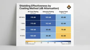
Performance data from industry testing:
| Coating System | Thickness | 100 MHz | 1 GHz | 5 GHz | 10 GHz |
|---|---|---|---|---|---|
| All-Over Plating | 1.0-10.0 µm | 108 dB | 120 dB | 113 dB | 87 dB |
| Selective Plating | 2.0-5.0 µm | 73 dB | 71 dB | 60 dB | 63 dB |
| Copper Paint | 0.025-0.375 mm | 63 dB | 70 dB | 81 dB | 63 dB |
Tradeoffs:
- Highest shielding effectiveness
- Excellent durability and wear resistance
- Requires more process steps and careful surface preparation
- Best suited to electroplateable plastics (ABS, ABS/PC)
- Higher capital and processing costs
How EMI Shielding Coatings Are Applied to Plastic Enclosures
Surface Preparation: The Foundation of Adhesion
Plastic surfaces must be thoroughly cleaned to remove mold release agents, oils, and contaminants. Chemical etching or plasma treatment follows to promote adhesion. Poor surface prep is the leading cause of coating delamination and shielding failure in production.
- No silicone or zinc stearate mold release agents if electroplating
- Plasma pre-treatment of 1 minute achieves excellent adhesion
- Cross-hatch adhesion testing per ASTM D3359 validates prep quality
Masking for Selective Coating
Before deposition, manufacturers mask areas that must remain uncoated. Common targets include exterior surfaces, connector interfaces, and snap-fit features. The masking method depends on geometry, volume, and coating process:
- Tape masking: Suitable for simple geometries and low-volume runs
- Wax plugs: Used for small ports, holes, and recessed connector openings
- Custom reusable fixtures: Preferred for high-volume production — improve consistency and cut labor cost
Providence Metallizing designs and builds precision masking fixtures in-house, enabling complex selective coating patterns that would be difficult to achieve reliably with tape alone.
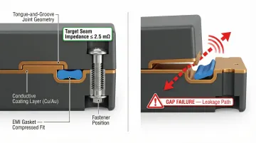
The Seam and Closure Challenge
The coating must extend right up to—and make continuous electrical contact at—the mating seams of enclosure halves. Gaps at seams are the primary EMI leakage path, and coating that stops short of the seam will not create a functional shield.
- Tongue-and-groove seam designs (both mating surfaces must be conductive)
- EMI gaskets to ensure conductive continuity across the joint
- Target seam impedance of 2.5 mΩ or less per SAE standard ARP 1481
Post-Coating Considerations
Once the shield coating is applied and seams are addressed, attention shifts to protecting the coating and verifying performance. Copper-based coatings in particular benefit from a protective topcoat to prevent oxidation over time. Quality assurance should include:
- Adhesion testing (tape peel, cross-hatch per ASTM D3359)
- Shielding effectiveness verification per relevant standards
- Visual inspection for coating uniformity and coverage
- Seam impedance measurement
Key Factors That Determine EMI Coating Effectiveness
Coating Material and Thickness
While coating conductivity matters, the primary driver of high-frequency shielding is ensuring continuous conductive closure with no gaps exceeding roughly 1/20th of the wavelength of the highest frequency of concern.
1 GHz example:
- Wavelength (λ) = 300 mm
- Maximum allowable gap = λ/20 = 15 mm
For a device with a 100 MHz clock generating harmonics up to 1 GHz, any seam gap larger than 15 mm will significantly degrade shielding effectiveness. This 1/20th wavelength rule provides approximately 20 dB of attenuation through the aperture.
Seam Integrity and Electrical Continuity
Even a well-applied coating will fail if enclosure halves don't make reliable conductive contact at every seam. Three common causes introduce micro-gaps that severely degrade shielding at higher frequencies:
- Inconsistent assembly pressure during closure
- Warped or out-of-tolerance plastic housing
- Insufficient fastener density along the seam length
The transfer impedance across the seam should be approximately 5 mΩ over the frequency range of interest, and it should not increase with time or aging.
Openings, Vents, and Cable Penetrations
Every aperture—ventilation holes, display windows, connector cutouts—is a potential leakage point. The maximum linear dimension, not the area, determines leakage.
Mitigation strategies:
- Honeycomb or mesh vent covers sized below critical wavelength
- Shielded cable entry points with 360-degree grounding
- Grounded connector backshells
- Conductive gaskets at panel interfaces
Substrate and Plastic Type
Not all plastics coat equally. ABS and ABS/PC are highly compatible with electroplating. Polycarbonate, nylon, Ultem, and other engineering thermoplastics may require specialized primers or surface activation.
Adhesion failures on difficult substrates are among the most common sources of EMI coating field failures when not validated during the design phase. Providence Metallizing has handled engineering-grade plastics including Ultem, Nylon, and LCP, using surface activation and etching pre-treatments validated against adhesion requirements before production begins.
How to Choose the Right EMI Shielding Coating Method
Decision Framework
For low-frequency shielding in standard consumer electronics:
- Conductive spray coatings may suffice
- Lower capital investment
- Faster prototyping and small-batch production
For high-frequency or military/medical applications requiring high shielding effectiveness:
- PVD sputtering or electroplating are preferred
- Superior uniformity and durability
- Better performance above 1 GHz
For complex geometries needing uniform coverage:
- Electroless plating or vacuum metallizing
- Reaches recessed areas and complex contours
- No line-of-sight limitations
For cost-sensitive, high-volume programs:
- Copper-nickel electroless/electroplate stack is the industry standard
- Optimizes performance, cost, and durability
- Scales efficiently to millions of units
Additional Selection Factors
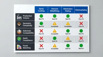
Five variables typically drive the final method decision:
- Production volume — Custom masking fixtures justify their cost at scale. High-volume systems can process over one million parts per week.
- Geometry complexity — Deep recesses, tight radii, and internal structures favor electroless plating or vacuum metallizing over spray coatings.
- Substrate compatibility — ABS and ABS/PC plate easily; polycarbonate, nylon, and engineering thermoplastics require specialized surface activation.
- RoHS compliance — All coating processes must meet EU RoHS Directive 2011/65/EU restricting lead, cadmium, mercury, hexavalent chromium, and other substances.
- Finish matching — Mixed-material assemblies often require consistent metallic appearance across plastic and metal components. Providence Metallizing, for example, maintains the capability to match finishes across both plastic and metal substrates — a practical advantage when appearance consistency matters across an entire assembly.
Qualification and Testing
Selecting the right method is only half the equation. Once a process is chosen, shielding effectiveness must be verified against relevant standards before moving to production:
- ASTM D4935: 30 MHz to 1.5 GHz for planar materials
- IEEE Std 299: 9 kHz to 18 GHz (extendable to 100 GHz) for shielding enclosures
- MIL-STD-285: Canceled in 1997; IEEE Std 299 is the replacement
Early involvement of the coating supplier during enclosure design reduces the risk of late-stage redesigns caused by seam issues or adhesion failures. Providence Metallizing offers free sampling for most applications, allowing engineers to validate shielding performance before committing to tooling and full production runs.
Frequently Asked Questions
What is EMI shielding?
EMI shielding is the use of conductive materials to block or attenuate electromagnetic interference, preventing unwanted signals from entering or escaping an electronic device. It protects the device and surrounding equipment from electromagnetic disruption.
What is an EMI coating?
An EMI coating is a conductive layer—spray paint, vacuum-deposited metal, or plated metal—applied to non-conductive surfaces like plastic to give them electromagnetic shielding properties by reflecting or absorbing electromagnetic energy.
Can plastic shield EMI?
Bare plastic offers no inherent EMI shielding because it is electromagnetically transparent. However, plastic enclosures become highly effective shields when conductive coatings (spray, vacuum metallizing, or plating) are applied to their interior surfaces.
What is the best material for EMI shielding?
Silver offers the highest conductivity, but copper-nickel combinations are most widely used for plastic enclosures. They balance shielding performance, corrosion resistance, cost, and process compatibility—making them the industry standard for most applications.
Are EMI and RF the same?
RF interference is a subset of EMI—all RFI is EMI, but EMI also covers lower-frequency conducted interference, electrostatic discharge, and power-line noise. RFI shielding specifically targets the radio-frequency band of that broader electromagnetic spectrum.
What's the difference between EMI and ESD?
EMI disrupts circuit operation through radiated or conducted electromagnetic fields; ESD is a sudden static charge transfer that can physically damage semiconductor components. Both threats often need addressing in enclosure design—and a single conductive coating can sometimes handle both.